1. AutomatedOpticalInspection(AOI)
Verifyinghigh-densityPCBcomponentsusingthe1.0xmagnificationandtelecentricopticstomaintainabsolutemeasurementintegrityacrossthesensorfield[1.1].
Problem SolvedPerspective errors in standard entocentric lenses cause false dimension failures on flat components. Telecentricity solves this by eliminating parallax.
AOITelecentricTV DistortionMachine Vision
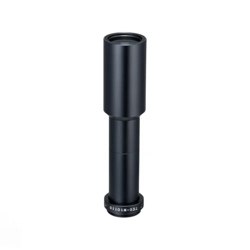
2. Precision Machining Metrology
Inspecting tight-tolerance micro-machined parts from exactly 111.5mm away, ensuring precise sub-millimeter measurements with -0.003% distortion.
Problem SolvedStandard lenses shift apparent object dimensions if part depth slightly varies on the inspection line, ruining exact metrology measurements.
MetrologyWorking DistanceDistortionC-Mount
3. Semiconductor Wafer Alignment
Providing consistent, high-contrast imaging of fiducial markers on silicon wafers by leveraging the 0.82mm depth of field and 6.9μm resolving power.
Problem SolvedTiny Z-axis height fluctuations during wafer positioning can defocus alignment markers or shift their apparent X/Y coordinates in conventional lenses.
SemiconductorWafer AlignmentResolving PowerDepth of Field