1. High-Precision Quality Control in Electronics Manufacturing
Inspection of tiny components, such as solder joints and PCB traces, on circuit boards for defects during the manufacturing process.
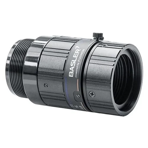
Problem SolvedThe lens's 5 MP resolution and 230 LP/mm capability allow for clear imaging of very small features (2.2 µm pixel size), enabling accurate detection of minute flaws that would be missed by lower-resolution optics. The 200mm minimum working distance facilitates close inspection without physical interference, crucial for micro-electronics.
Machine VisionPCB InspectionSolder Joint InspectionHigh ResolutionMicro-inspection
2. Automated Medical Device Assembly and Inspection
Automated assembly and inspection of small medical device components, such as catheters or surgical tools, requiring precise alignment and defect detection in controlled environments.
Problem SolvedThe lens's high resolution and minimal distortion ensure accurate measurement and inspection of critical dimensions and surface imperfections on small, intricate medical parts. The robust metal housing and locking screws provide essential stability in cleanroom or vibratory manufacturing environments, maintaining image integrity.
Medical Device ManufacturingAutomated InspectionPrecision AssemblyQuality AssuranceSmall Part Inspection
3. Material Surface Analysis and Defect Detection
Detailed examination of material surfaces (e.g., metals, ceramics, textiles) for scratches, cracks, or structural irregularities in industrial quality control and research.
Problem SolvedThe lens's ability to render crisp images with high contrast and low distortion is crucial for reliably identifying subtle surface defects or textural variations. Its fixed 12mm focal length provides a consistent field of view for repetitive, standardized inspection tasks across various materials.
Surface InspectionMaterial ScienceDefect DetectionQuality ControlMicro-structure Analysis