1. Automated BGA (Ball Grid Array) Solder Joint Inspection
Utilizing the IDS U3-34L0CP camera to inspect highly reflective BGA solder balls against dark PCB substrates during surface-mount technology (SMT) electronics manufacturing.
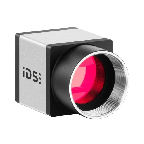
Problem SolvedExtreme contrast between shiny solder joints and dark substrates causes standard sensors to lose critical micro-defect details in shadows or highlights. The U3-34L0CP's IMX676 sensor manages these high-contrast scenes effectively, while its 12.62 MP resolution and ultra-fine 2.00 µm pixel size capture micro-scale defects like solder bridging or voids. The 5.00 Gbps USB 3 interface ensures fast 31.9 fps throughput for inline inspection, and the IP30 rating is perfectly suited for dry, cleanroom PCB manufacturing environments [1.7].
BGA inspection12.62 MP resolution2.00 µm pixel sizeUSB 3 (5.00 Gbps)IP30 ratingSony IMX676 CMOS
2. High-Resolution Digital Pathology & Automated Microscopy
Integrating the camera into automated digital slide scanners and microscopes to digitize biological tissue samples, biopsy slides, and cell cultures in lab automation systems.
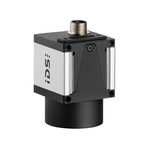
Problem SolvedStandard rectangular sensors waste the circular optical field of view produced by microscope lenses, requiring more mechanical step-and-scan movements to digitize a full slide. The camera solves this with its 3552 x 3552 square pixel array (7.104 mm x 7.104 mm optical area), perfectly matching round lenses for uniform, format-filling image projection. The ultra-compact 29 x 29 x 29 mm housing allows easy integration into tight optomechanical instrument spaces, while the rolling shutter is optimal for capturing stationary specimens with extremely high fidelity.
Automated microscopySquare sensor format3552 x 3552 resolution7.104 mm optical area29 x 29 x 29 mm dimensionsRolling Shutter
3. Semiconductor Wafer Surface Defect Inspection
Deploying the vision system on automated wafer-handling robotic stages to perform step-and-scan detection of microscopic scratches, particles, and coating anomalies on silicon wafers.
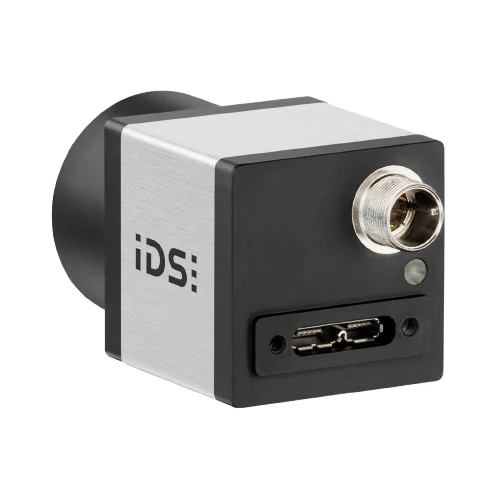
Problem SolvedDetecting micron-level defects on highly reflective semiconductor wafers requires immense pixel density, but space constraints on robotic handlers restrict camera size. The camera's 2.00 µm pixel size and 12.62 MP resolution reliably resolve microscopic anomalies across a wide 2/3" optical class area. Its miniature 29 x 29 x 29 mm footprint easily mounts on tight robotic arms. The fast 31.9 fps frame rate at maximum resolution over a 5.00 Gbps USB 3 interface maximizes wafer throughput without bottlenecking the system.
Wafer inspectionSurface defect detection2.00 µm pixel size31.9 fps frame rate2/3" optical classCompact 29x29x29 mm